MENA SC 2023: Exploring the Latest Developments in Silicon Photovoltaic-Based Technologies

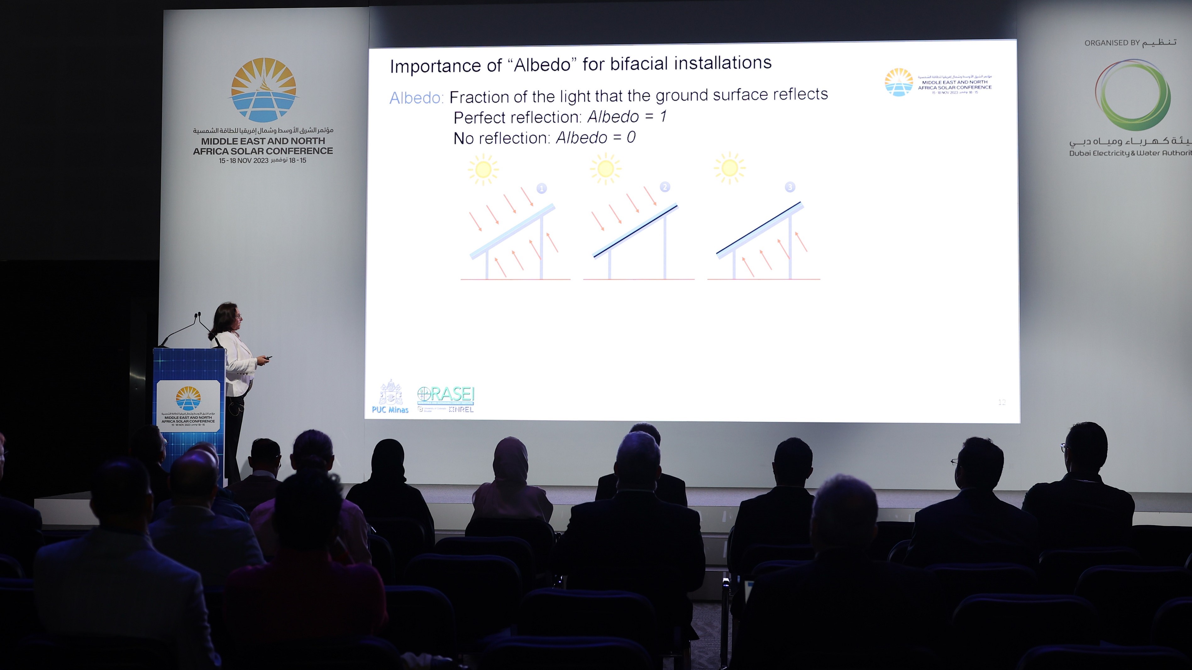
Dubai, UAE, 18 November 2023: The research papers at the first Middle East and North Africa Solar Conference (MENA SC) discussed the latest solar photovoltaic updates, innovations and technologies. Prominent global speakers, researchers, scientists and specialists, focused on improving the performance and efficiency of silicon photovoltaic systems, and cost reduction. Dubai Electricity and Water Authority (DEWA) organised MENA SC, the first scientific and technical conference of its kind in the region, specialising in solar energy systems, from 15 to 18 November 2023 at the Dubai World Trade Centre.
“We are committed to achieving the directives of His Highness Sheikh Mohammed bin Rashid Al Maktoum, Vice President and Prime Minister of the UAE and Ruler of Dubai, to enhance the position of the UAE on the top of the list in competitiveness in solar energy, and among the top ten countries in energy efficiency. We also work to promote Dubai as a platform for innovation, a destination for creators and an incubator for innovators from all over the world. As innovation in clean and renewable energy accelerates, we attach great importance to research and development, and we encourage green investments to keep pace with the changes and developments. This increases our effective contribution in forecasting and shaping a sustainable future. This also supports the Dubai Net Zero Carbon Emissions Strategy 2050, to provide 100% of Dubai’s total power capacity from clean energy sources by 2050,” said HE Saeed Mohammed Al Tayer, MD & CEO of DEWA.
The research papers at the conference focused on a wide range of topics, including unconventional and new concepts for future technologies; silicon photovoltaic materials and devices; Perovskite and organic materials and solar cells; PV module and system reliability in MENA region; solar resources for PV and forecasting; power electronics and grid integration; and all of which are key in accelerating the green energy transformation.
Silicon Photovoltaic Materials and Devices
MENA SC highlighted the best ways and materials to develop the manufacturing of silicon photovoltaic panels, and improve the quality of silicon wafers. This aims to increase their efficiency to produce more energy at a minimal cost. The conference covered all areas of the silicon solar field, ranging from silicon purity to thin-film deposition, from electronic transport through new contact structures to high-efficiency devices, from light management to loss analysis, and from interconnection to module field degradation caused by cell deterioration.
Silicon Material, Interconnection and Module Integration
The research papers highlighted all aspects related to treating and producing silicon material including crystallisation, wafering, slicing technologies and alternative methods to produce silicon wafers. They also discussed the mechanical and electrical characteristics of the resulting wafers and their impact on device performance, including material changes during subsequent processing and defect engineering steps. They also highlighted techniques for electrode formation, mechanical adhesion, multi-wire technologies, and the interconnection of advanced cell structures. The conference also focused on contacts formed on silicon absorbers, and specifically those layers that passivate the absorber surface. It also highlighted device physics and characterisation of contacts, the properties of new contact materials, and the performance of cells with contact layers such as amorphous silicon, polysilicon, and metal oxides.
Device Physics, Simulation and New Characterisation Techniques
The sessions at MENA SC focused on understanding, quantifying, and modelling phenomena in silicon solar cells, including new interpretations of device physics, multi-dimensional models, numerical analysis of novel cell concepts, power loss measurement and mitigation strategies, computational simulations, and associated means of validation. The sessions also focused on the development of new device characterisation techniques, which may be based on photoluminescence or capacitance measurements. They also covered light management within silicon solar cells, thin film silicon, surface engineering of silicon cells to increase photon, as well as approaches to reduce front-surface reflectance and parasitic absorption.


